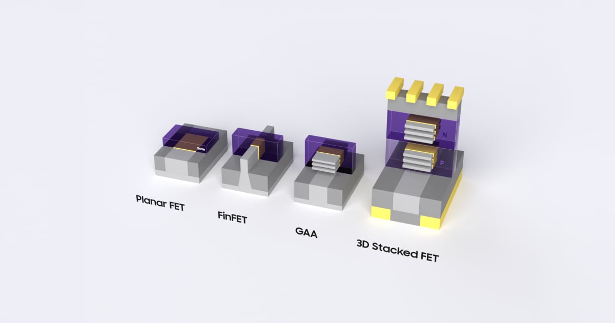
Samsung Demonstrates 3D Stacked FETs with Triple Nanosheet Channels at 42nm
Samsung has successfully demonstrated 3D Stacked FETs with triple nanosheet channels at 42nm, achieving a breakthrough in transistor density by vertically stacking n-type and p-type transistors rather than placing them side-by-side, enabling significantly more processing power within the same chip footprint. This advancement represents the natural evolution of semiconductor architecture and addresses the physical limitations of traditional planar designs, directly impacting the performance and power efficiency capabilities of next-generation computing devices that IT organizations will deploy. For technology leaders, this signals that Samsung's roadmap will deliver higher computational density and efficiency gains in future processors, requiring IT infrastructure planning to account for improved performance characteristics and potentially shifted thermal and power management profiles.